Serial Peripheral Interface
This example will use an analog to digital converter to read the analog voltage across a photoresistor. A photoresistor decreases resistance (and the voltage across it) when it is exposed to light.
The Serial Peripheral Interface (SPI) is a communication protocol used to transfer data between micro-computers like the Raspberry Pi and peripheral devices. These peripheral devices may be either sensors or actuators. In this example, we will be learning to use an Analog to Digital Converter (ADC) sensor. An analog to digital sensor takes an analog voltage and converts it into a digital number that can be understood by the Raspberry Pi.
SPI uses 4 separate connections to communicate with the target device. These connections are the serial clock (CLK), Master Input Slave Output (MISO), Master Output Slave Input (MOSI) and Chip Select (CS).
- The clock pin sense pulses at a regular frequency, the speed at which the Raspberry Pi and SPI device agree to transfer data to each other. For the ADC, clock pulses are sampled on their rising edge, on the transition from low to high.
- The MISO pin is a data pin used for the master (in this case the Raspberry Pi) to receive data from the ADC. Data is read from the bus after every clock pulse.
- The MOSI pin sends data from the Raspberry Pi to the ADC. The ADC will take the value of the bus on the rising edge of the clock. This means the value must be set before the clock is pulsed.
- Finally, the Chip Select line chooses which particular SPI device is in use. If there are multiple SPI devices, they can all share the same CLK, MOSI, and MISO. However, only the selected device has the Chip Select line set low, while all other devices have their CS lines set high. A high Chip Select line tells the SPI device to ignore all of the commands and traffic on the rest of the bus.
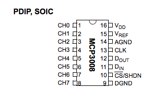
The ADC used in this example is the MCP3008. It is an 8-channel, 10-bit analog to digital converter. The 8-channel part means that it can accept up to 8 different analog voltages, however it can only convert one voltage at any one time. The 10-bit property is the resolution of the ADC, or the precision to which it can measure a voltage. The range of analog voltages is represented as a 10-bit number on the output. If the ADC is measuring voltages from 0-3.3V, each step in the output value represents a change of .003 volts.
Setting up Raspbian Wheezy for SPI
Comment out the spi-bcm2708 line in the raspi-blacklist.conf file
 sudo nano /etc/modprobe.d/raspi-blacklist.conf
#blacklist spi-bcm2708

sudo modprobe spi_bcm2708
Hardware Implementation
Hardware SPI Connections
There is a kernel module that can make use of the Raspberry Pi's built in SPI support. This requires the spidev module. Check if you have it loaded by running 'lsmod | grep spi'. If the module is present, this should be the output
  pi@pi-friedrich /sys/class/gpio/gpio18 $ lsmod | grep spi
    spidev                  5600  0
    spi_bcm2708             5386  0
If you don't have the module running, you'll need to install it: First, install python development headers:
sudo apt-get update sudo apt-get install python-dev
git clone git://github.com/doceme/py-spidev
cd py-spidev
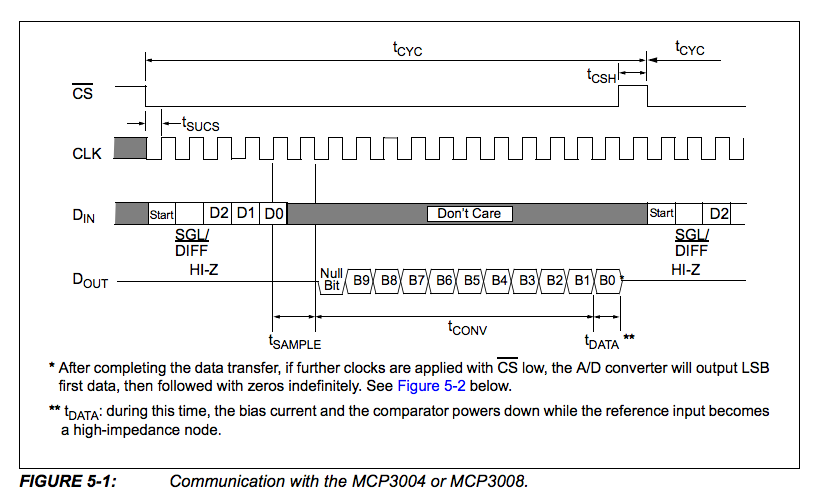
sudo python setup.py installThe spidev module, just like RPi.GPIO needs root permissions to read/write the SPI device driver: spidev.open(bus, dev) Raspberry Pi has 1 buses (#0), 2 devices. They share the same CLK, MOSI, and MISO, but have different chip selects (CE0, CE1) There are basic read and write commands (readbytes() and writebytes()). There are also commands for SPI transaction(combined read and write, like we are doing here) These are xfer() and xfer2(). xfer() re-asserts CS after each byte, while xfer2() keeps CS asserted for the whole transaction (what we want) For both xfer() and xfer2(), every byte written on the bus results in a byte read back from the SPI device. Looking at the timing chart above, we write 5 bits to the device and then read 12 bits back. The lowest 10 bits of those 12 bits are the result. As the xfer() functions work in bytes, those 17 bits mean we need to use 3 bytes(24 bits) total. The first 7 bits of the read and write are ignored.
Sample Code - Fill in the blanks

#!/usr/bin/env python
#
# Bitbang'd SPI interface with an MCP3008 ADC device
# MCP3008 is 8-channel 10-bit analog to digital converter
#  Connections are:
#     CLK => SCLK
#     DOUT =>  MISO
#     DIN => MOSI
#     CS => CE0

import time
import sys
import spidev

spi = spidev.SpiDev()
spi.open(0,0)

def buildReadCommand(channel):
    startBit = 0x01
    singleEnded = 0x08

    # Return python list of 3 bytes
    #   Build a python list using [1, 2, 3]
    #   First byte is the start bit
    #   Second byte contains single ended along with channel #
    #   3rd byte is 0
    return []

def processAdcValue(result):
    '''Take in result as array of three bytes.
       Return the two lowest bits of the 2nd byte and
       all of the third byte'''
    pass

def readAdc(channel):
    if ((channel > 7) or (channel < 0)):
        return -1
    r = spi.xfer2(buildReadCommand(channel))
    return processAdcValue(r)

if __name__ == '__main__':
    try:
        while True:
            val = readAdc(0)
            print "ADC Result: ", str(val)
            time.sleep(5)
    except KeyboardInterrupt:
        spi.close()
sys.exit(0)Our first bitbang'd implementation (More difficult)
Here is how the analog to digital converter works:
- Make sure the CS line is set high, clock pin low, and MOSI pin Low
- Issue a command to the ADC to read a value from a particular input (in the example, channel 0) a) Set the CS line low to start the command. b) Send 5 bits to the ADC: a start bit, followed by a command bit, then the channel number. The bit should be set on the MOSI pin before the clock pulse for each of the 5 bits
- Read the value back from the DC. a) Pulse the clock 12 times, each time reading the value from the MISO pin. b) The first bit is a an empty bit, followed by a NULL bit (which can be ignored). The next 10 bits are the digital value.
- Set the CS line low to end the transaction
The Raspberry Pi can speak SPI in two ways, bit banging and support from a hardware driver. Bitbanging means manually driving the clock pulses and data lines from your program. It requires a more detailed knowledge of the protocol so is great for learning more about SPI.
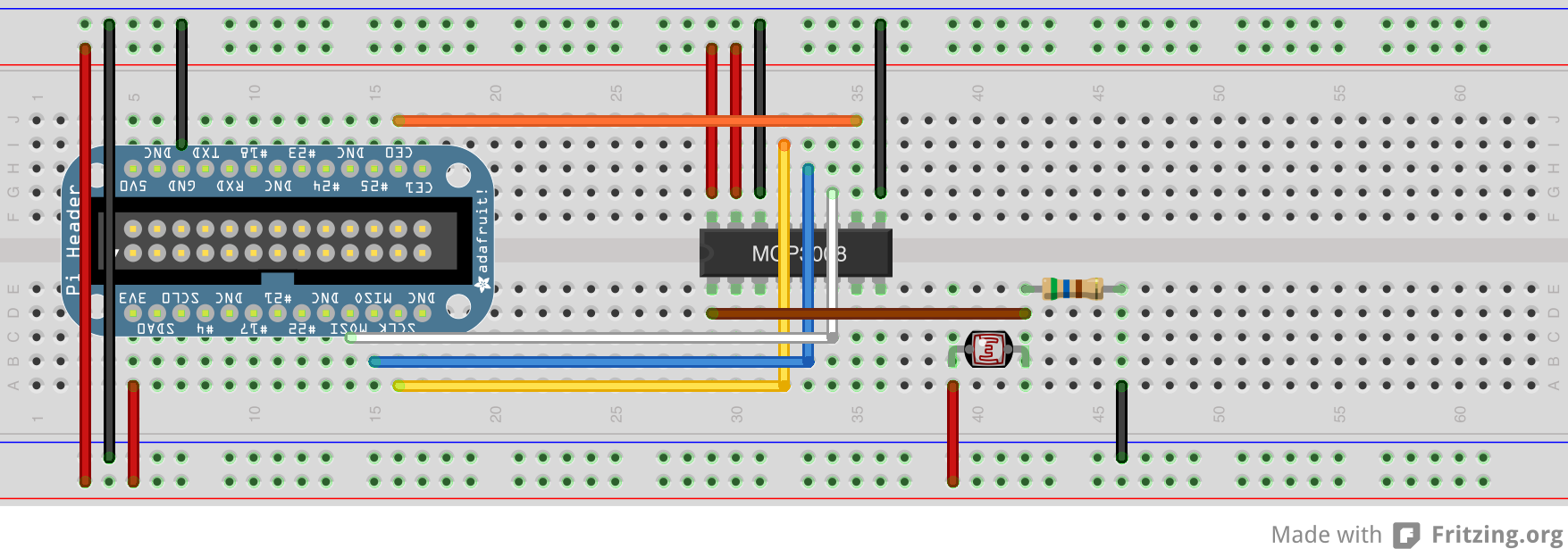
Connecting the ADC to the Raspberry Pi uses 4 standard GPIO Ports. Here we connect as follows:
- GPIO Pin 18 => CLK
- GPIO Pin 23 => Raspberry Pi MISO, ADC DOUT
- GPIO Pin 24 => Raspberry Pi MOSI, ADC DIN
- GPIO PIn 25 => Chip Select (active low)
Software SPI Connections
We'll be measuring the voltage across a photo resistor to measure light levels. A photo resistor's resistance decreases under bright light. In our circuit, this will cause the voltage at the input of the ADC to increase. Brighter light, higher voltage. In this circuit, we are using 3.3V as our Reference Voltage. This is the highest voltage we can convert. If we wanted to, we could connect VRef to 5V and then convert voltages up to 5V.
Sample Code- Fill in the blanks
#!/usr/bin/env python
#
# Bitbang'd SPI interface with an MCP3008 ADC device
# MCP3008 is 8-channel 10-bit analog to digital converter
#  Connections are:
#     CLK => 18
#     DOUT => 23 (chip's data out, RPi's MISO)
#     DIN => 24  (chip's data in, RPi's MOSI)
#     CS => 25

import RPi.GPIO as GPIO
import time
import sys

CLK = 18
MISO = 23
MOSI = 24
CS = 25

def setupSpiPins(clkPin, misoPin, mosiPin, csPin):
    ''' Set all pins as an output except MISO (Master Input, Slave Output)'''
    pass

def readAdc(channel, clkPin, misoPin, mosiPin, csPin):
    if (channel < 0) or (channel > 7):
        print "Invalid ADC Channel number, must be between [0,7]"
        return -1

    # Datasheet says chip select must be pulled high between conversions


    # Start the read with both clock and chip select low


    # read command is:
    # start bit = 1
    # single-ended comparison = 1 (vs. pseudo-differential)
    # channel num bit 2
    # channel num bit 1
    # channel num bit 0 (LSB)
    read_command = 0x18
    read_command |= channel

    sendBits(read_command, 5, clkPin, mosiPin)

    adcValue = recvBits(12, clkPin, misoPin)

    # Set chip select high to end the read


    return adcValue

def sendBits(data, numBits, clkPin, mosiPin):
    ''' Sends 1 Byte or less of data'''

    data <<= (8 - numBits)

    for bit in range(numBits):
    pass
        # Set RPi's output pin high or low depending on highest bit of data field

        # Advance data to the next bit

        # Pulse the clock pin HIGH then immediately low


def recvBits(numBits, clkPin, misoPin):
    '''Receives arbitrary number of bits'''
    retVal = 0

    # For each bit to receive
        # Pulse clock pin high then immediately low

        # Read 1 data bit in and include in retVal

        # Advance input to next bit

    # Divide by two to drop the NULL bit
    return (retVal/2)


if __name__ == '__main__':
    try:
        GPIO.setmode(GPIO.BCM)
        setupSpiPins(CLK, MISO, MOSI, CS)

        while True:
            val = readAdc(0, CLK, MISO, MOSI, CS)
            print "ADC Result: ", str(val)
            time.sleep(5)
    except KeyboardInterrupt:
        GPIO.cleanup()
        sys.exit(0)